June 08, 2026
In the previous article, we wrote some random data to the ROM using an Arduino Mega 2560 and read it back. We are going to take things further. The Arduino will still flash the ROM, but once that's done we are going to place the ROM in our Frankenstrad, and not only the Z80 will read it, it will also execute the code it contains. The code is going to be simple, it will read data from the ROM and write it back in RAM.
Since we are about to write data in RAM, we need to setup our system so that the ROM and the RAM can coexist and share the same 64 KB address space.
From the Z80 perspective, there is no difference between ROM and RAM; it just accesses memory in the range [0000:FFFF]. It doesn't know which kind of memory it accesses at these addresses, nor does it care. It is the CPC gate array's responsibility to select the right chip depending on which ROM bank has been enabled and the state of address lines 14 and 15.
For now, we will only use the lower 16 KB that will be mapped to [0000:3FFF]. Higher addresses will be mapped to the RAM, emulated by the ESP32.
+---------------------+ FFFFh
|                     |
|                     |
| RAM - 48 KB         | 8000h
|                     |
|                     |
+---------------------+ 4000h
| ROM - 16 KB         |
+---------------------+ 0000h
Whenever an address of at least 4000h is present on the bus, we need to disable the ROM and enable the RAM instead. For addresses lesser than 4000h, we will do the opposite.
/CE. Any address of at least 4000h will have one of these two bits on, and since the chip enable signal is active low, this will disable the ROM.4000h on the address bus, effectively disabling the RAM.void IRAM_ATTR on_z80_clock()
{
z80_clock_state = 1 - z80_clock_state;
gpio_set_level(GPIO_Z80_CLOCK, z80_clock_state);
if (z80_clock_state == LOW)
{
// Falling edge of the clock: sample the address bus
address_bus = 0;
int shift = 0;
for (const auto line : address_lines)
{
address_bus |= gpio_get_level(line) << shift;
shift ++;
}
}
else
{
// Rising edge of the clock
if (gpio_get_level(GPIO_Z80_RD) == LOW)
{
if (address_bus >= 0x4000)
{
// Reading from the RAM
uint8_t data = memory[address_bus];
for (const auto pin : data_lines)
{
gpio_set_direction(pin, GPIO_MODE_OUTPUT);
digitalWrite(pin, data & 0x1);
data >>= 1;
}
}
else
{
// Reading from the ROM
for (const auto pin : data_lines)
{
gpio_set_direction(pin, GPIO_MODE_DISABLE);
}
}
}
else if (gpio_get_level(GPIO_Z80_WR) == LOW)
{
uint8_t data = 0;
int32_t shift = 0;
for (const auto pin : data_lines)
{
gpio_set_direction(pin, GPIO_MODE_INPUT);
data |= digitalRead(pin) << shift;
shift++;
}
memory[address_bus] = data;
}
}
}
We'll reuse almost the same code we used to test the Z80 with a few modifications. The code still starts at address 0000h and the source string still lives at address 0010h, but this time on the ROM instead of the simulated RAM in the ESP32. Since the destination buffer will be in RAM, we'll set it at 4000h. This is the new code:
LD HL, 0010h    ;Address of the string to copy
LD DE, 4000h    ;Address of destination buffer
LD BC, 12h      ;Length of data string
LDIR            ;Move String
HALT            ;Stop here
And this is the corresponding byte code, which includes some padding so that the data starts at address 0010h:
const uint8_t rom[] =
{
    // Code
    0x21, 0x10, 0x00,       // LD HL, 0010h
    0x11, 0x00, 0x40,       // LD DE, 4000h
    0x01, 0x12, 0x00,       // LD BC, 0012h
    0xED, 0xB0,             // LDIR
    0x76,                   // HALT

    // Padding
    0x00, 0x00, 0x00, 0x00,

    // Source Data "Frankenstrad 6128"
    0x46, 0x72, 0x61, 0x6E, 0x6B, 0x65, 0x6E, 0x73, 0x74, 0x72, 0x61, 0x64, 0x20, 0x36, 0x31, 0x32, 0x38, 0x00
};
And now we just have to program this few bytes to our flash memory with our home-made ROM flasher.
So far, the Z80 was only talking with the ESP32. Now we're throwing a third chip into the mix. And down the road we will be adding a number of other things to our system. We need to be smart about this. We have 8 lines of data, 16 lines of addresses, a few control signals, and most of these need to go across the whole system. This can quickly escalate into a big mess of tangled wires extremely difficult to work with.
Here is what matters to me:
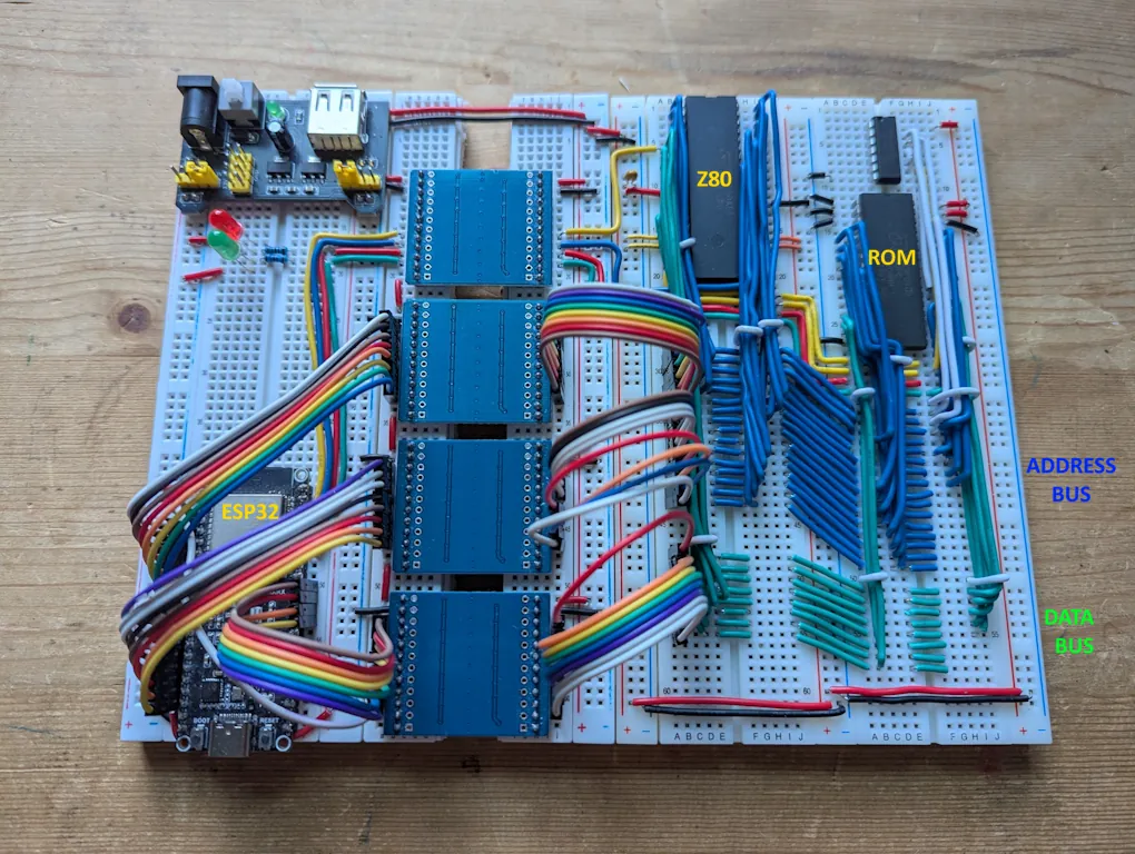
With all that in mind, here is where the Frankenstrad is at:
I'm trying to keep an area for the buses and signals that will probably keep going all the way through the system. From the buses, I'm branching off wires to the chips. Since these "branches" lie along the boards rather than across, there isn't a lot of space. I build them vertically, stacking wires together to leave room. So far, so good!
Powering the system up, it reads the string from the ROM and writes it to the RAM. It doesn't look like much, we were already doing something very similar an article ago. Except that this time, the Z80 is asking the ROM what to do, the ROM answers, and the CPU does it. And watching these two talk to each other to do something together is pretty magical. They grow up so fast!...
Next, let's add some RAM to our system instead of emulating it! The duo will become a trio and this chippy dialog a discussion.