May 22, 2026
Well, well, well! Look who decided to show up! If it isn't the new Z80 we've been waiting for!
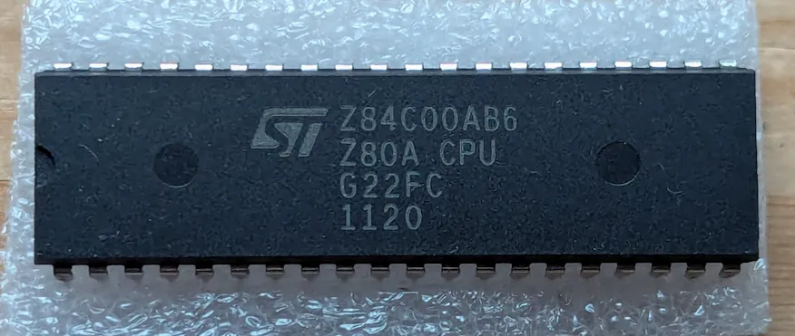
Z84C00AB6: Z84C00 means it is the CMOS version of the Z80 ; A means the clock can go up to 4 MHz, B6 means it is in a plastic package.Z80ACPU: it's a 4 MHz Z80 CPU.1120: it was manufactured during the 20th week of 2011.First things first, to the test board! We know the drill: plug it onto the test board which is wired to the Arduino Mega that will run the test. The same test we've used before on the older NMOS Z80, running an infinite repetition of NOP instructions to verify that our machine cycles are sound. And, as expected, all is well.
Let's take things a bit further. Instead of executing NOP instructions ad nauseam, let's try one of the instruction examples from the Z80 user manual. The first example is a string transfer. It is simple and will force us to learn how to read and write back bytes in memory. We've already figured out the machine cycles, now is the time to figure out the read and the write cycles.
Here is the listing, it copies a 737-byte string from the address DATA to the address BUFFER.
LD HL, DATA     ;START ADDRESS OF DATA STRING
LD DE, BUFFER   ;START ADDRESS OF TARGET BUFFER
LD BC, 737      ;LENGTH OF DATA STRING
LDIR            ;MOVE STRING–TRANSFER MEMORY POINTED
                ;TO BY HL INTO MEMORY LOCATION POINTED
                ;TO BY DE INCREMENT HL AND DE,
                ;DECREMENT BC PROCESS UNTIL BC = 0
We have to convert this code into byte code and store it on the Arduino. The Arduino will send it to the Z80, one byte at a time. It will also fake the memory to hold the string data and the destination buffer. We are going to modify this example to use a shorter string, Frankenstrad 6128, which is 18 bytes long. We will also add an extra instruction at the end to halt execution.
To store the code and the data, the Arduino is going to fake the memory. This is a simple C array big enough to host a code segment and a data segment. The code will need 12 bytes, and the data 36 bytes to store both buffers. Let's round up these numbers for good measure to 16 bytes for code and 48 bytes for data. 64 bytes total.
uint8_t memory[64];
uint16_t code_segment = 0;
uint16_t data_segment = 16;
uint16_t source_address = data_segment;
uint16_t destination_address = source_address + 24;

void setup()
{
    strcpy(&memory[source_address], "Frankenstrad 6128");
    strcpy(&memory[destination_address], ".................");
}
With all that in mind, let's modify the example:
DATA is where the string data is. In the C code, it lives at the beginning of the data segment, at address 16 (10h in hexadecimal).BUFFER is the destination buffer. In the C code, it is 24 bytes after the start of the data segment, at address 40 (28h).737 was the length in the original example. We replaced it with a length of only 18 (12h).HALT instruction at the end to stop the execution and avoid interpreting our data segment as code and try to execute it.LD HL, 10h ;Start address of source
LD DE, 28h ;Start address of destination
LD BC, 12h ;Length of data string
LDIR ;Move String
HALT ;Stop here (so that we don't try execute what is in the data segment)
Let's translate this into byte code.
The LD instructions load 16-bit values (the second operands) into a pair of 8-bit registers (the first operands). The first operand is embedded in the first byte of the op code.
| Destination | Op Code |
|---|---|
| BC | 01h |
| DE | 11h |
| HL | 21h |
The second operand, the 16-bit value, is split into the two next bytes of the op code, low-order byte first.
| Instruction | Op Code |
|---|---|
LD HL, 0010h |
21 10 00 |
LD DE, 0028h |
11 28 00 |
LD BC, 0012h |
01 12 00 |
Next is the LDIR instruction. It has no operand and its op code is EDB0h.
And finally we have the HALT instruction, whose op code is a single byte 76h.
We have all our 12 bytes of code to populate our code segment. Since our code segment is conveniently mapped at the address 0000, we can just initialize our memory with it. The data will be mapped after that at address 16.
uint8_t memory[64] =
{
    0x21, 0x10, 0x00,   // LD HL, 0010h
    0x11, 0x28, 0x00,   // LD DE, 0028h
    0x01, 0x12, 0x00,   // LD BC, 0012h
    0xed, 0xb0,         // LDIR
    0x76                // HALT
};
We byte code is ready to be sent to the Z80, now we need to determine when to send it. In part 2, we were sampling the address lines on the falling edge of the clock while the read signal was active. We knew that time to be safe to read the program counter only once per machine cycle. But now things are different. Whatever we do must be valid not only for the machine cycle, but also for the read and write cycles. What really matters to us now is to know when we should access the data bus to meet the CPU requests.
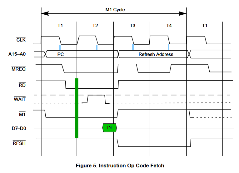
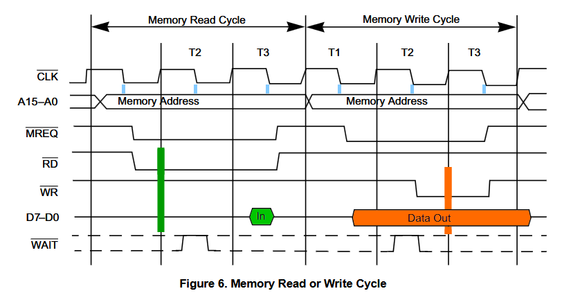
Looking at these two diagrams, the falling edge of the clock, in blue, looks like a good moment to sample the address bus. Once it's been sampled by the Arduino, we can use it to read or write the data bus on the rising edge of the clock. If the read signal is active, on the green lines, we can write the data we have in memory onto the data bus to serve it to CPU. Likewise, if the write signal is active, on the orange line, we can sample the data bus, filled by the CPU, and store it in our memory.
So really, all we need to do is sample the address bus on the falling edge of the clock and access the data bus as needed on the rising edge of the clock. I like how simple this is on the Arduino, almost mechanical.
void loop()
{
    // Keep track of the time
    uint32_t half_clock_period_end = micros() + clock_period_in_us/2;

    // Rising edge of the clock
    digitalWrite(clock_pin, HIGH);

    // Check if the CPU wants to read data from memory
    if (digitalRead(read_pin) == LOW)
    {
        write_data_lines(memory[address_bus]);

        print_format("Reading [%04x] %02x", address_bus, memory[address_bus]);
    }

    // Check if the CPU wants to write data to memory
    if (digitalRead(write_pin) == LOW)
    {
        memory[address_bus] = read_data_lines();

        print_format("Writing [%04x] %02x", address_bus, memory[address_bus]);
        print_format("%16s -> %16s", (char*)&memory[source_address], (char*)&memory[destination_address]);
    }

    // Wait until the end of the half clock period
    while (micros() < half_clock_period_end)
    {
        yield();
    }
    half_clock_period_end = micros() + clock_period_in_us/2;

    // Falling edge of the clock
    digitalWrite(clock_pin, LOW);

    // Sample the address bus
    address_bus = read_address_lines();

    // Wait until the end of the clock period
    while (micros() < half_clock_period_end)
    {
        yield();
    }
}
And here we go, the string is getting copied!
Initializing pins
Reset Sequence
Ready
SRC 'Frankenstrad 6128'
DST '.................'
Reading [0000] 21
Reading [0001] 10
Reading [0002] 00
Reading [0003] 11
Reading [0004] 28
Reading [0005] 00
Reading [0006] 01
Reading [0007] 12
Reading [0008] 00
Reading [0009] ed
Reading [000a] b0
Reading [0010] 46
Writing [0028] 46
Frankenstrad 6128 -> F................
Reading [0009] ed
Reading [000a] b0
Reading [0011] 72
Writing [0029] 72
Frankenstrad 6128 -> Fr...............
Reading [0009] ed
Reading [000a] b0
Reading [0012] 61
Writing [002a] 61
Frankenstrad 6128 -> Fra..............
Reading [0009] ed
Reading [000a] b0
Reading [0013] 6e
Writing [002b] 6e
Frankenstrad 6128 -> Fran.............
Reading [0009] ed
Reading [000a] b0
Reading [0014] 6b
Writing [002c] 6b
Frankenstrad 6128 -> Frank............
Reading [0009] ed
Reading [000a] b0
Reading [0015] 65
Writing [002d] 65
Frankenstrad 6128 -> Franke...........
Reading [0009] ed
Reading [000a] b0
Reading [0016] 6e
Writing [002e] 6e
...
Frankenstrad 6128 -> Frankenstrad 61..
Reading [0009] ed
Reading [000a] b0
Reading [001f] 32
Writing [0037] 32
Frankenstrad 6128 -> Frankenstrad 612.
Reading [0009] ed
Reading [000a] b0
Reading [0020] 38
Writing [0038] 38
Frankenstrad 6128 -> Frankenstrad 6128
Reading [0009] ed
Reading [000a] b0
Reading [0021] 00
Writing [0039] 00
Frankenstrad 6128 -> Frankenstrad 6128
Reading [000b] 76
Reading [000c] 00
It is... beautiful! Time to pop the Z80 out of the testing board and take it to the "real" board. We are also going to carry over these new timings to the ESP32 code to sample the address and data bus.
And this concludes our testings of the Z80. Actually, we think we've been testing the Z80 but, really, the Z80 has been testing us. The CPU had no problem doing its thing, we did! We were the test subjects all along, and I'm glad to see that we've passed the test. We are worthy to continue!
What's next? We grab the ROM from the CPC 6128, dump it onto our EEPROM, run it, and get the Ready screen.