June 08, 2026
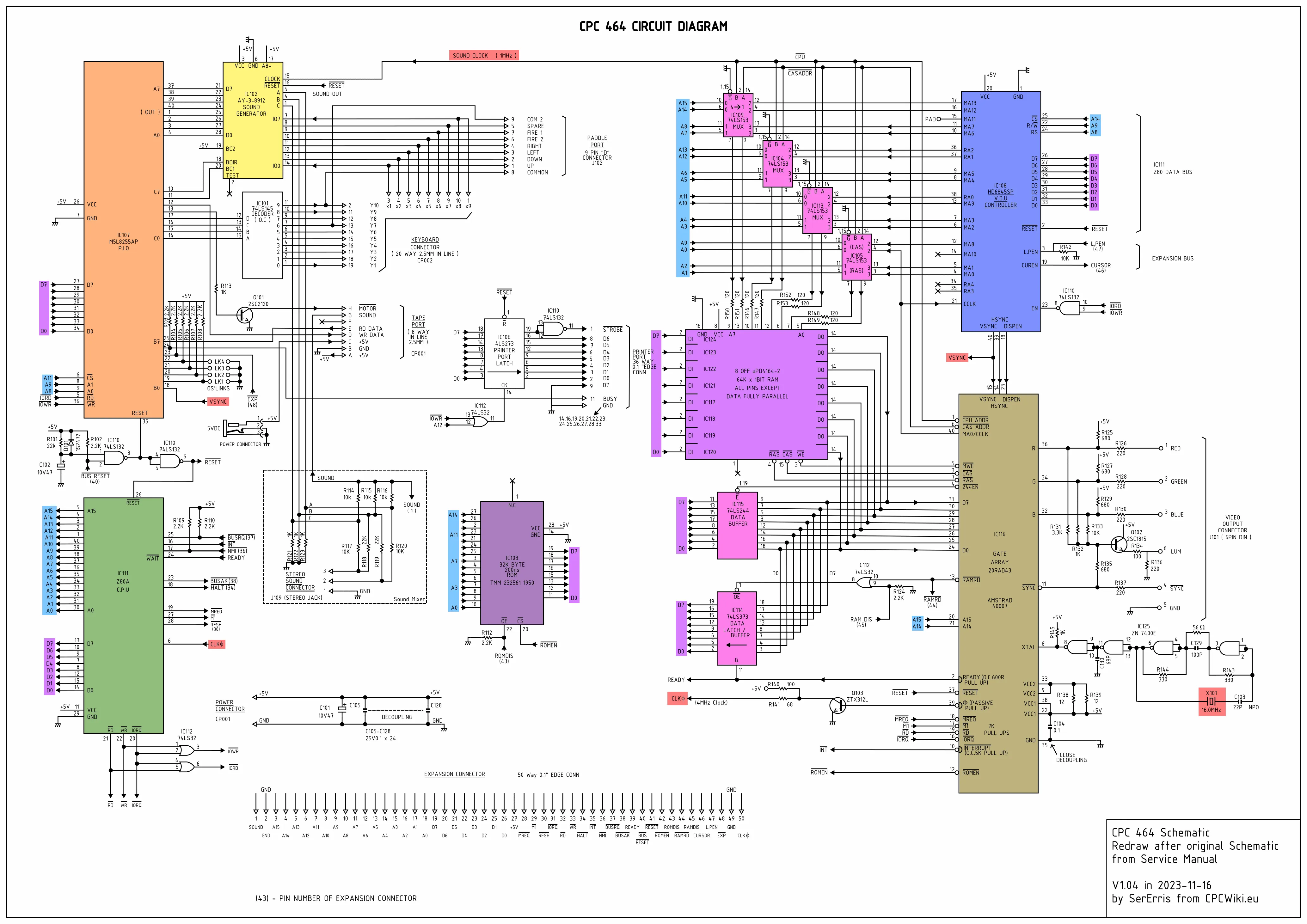
The ROM (Read-Only Memory) in the original CPC 464 seems to be a TMM 232561 1950. I've looked it up but could not find what the chip actually is. We can still gather info from the 464 circuit diagram. We can see that it is a 32 KB ROM with an access time of 200 ns. It has 15 address lines, 8 data lines, a chip enable signal and an output enable signal.
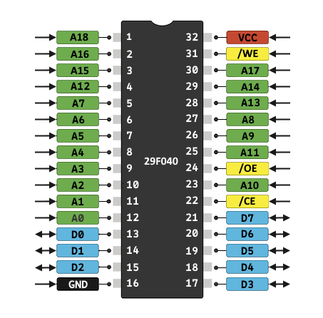
For our purpose, we need an EEPROM, so that we can erase it and reprogram it with the system BIOS as needed. Reprogramming it is also nice if we to bring some modifications to the BIOS. I could not find an EEPROM that meets the few criteria that we have, but I found a flash memory device, the Am29F040B. It holds 512 KB with an access time of 90 ns. This is plenty! We can actually have different versions of the BIOS at the same time if we want and switch between them with a toggle switch or something. Or maybe go crazy and expand the ROM size with new BIOS functionalities!
Back to reality, we first need to program our ROM. I do not have a ROM programmer. But I have my trusty Arduino Mega 2560, a bunch of wires, and the Am29F040B datasheet.
There are a couple of things we need to know about flash memory. It can be erased, programmed (written to), and of course, read. The memory is made of 8 sectors of 64 KB. Erasing is done block-wise, not byte-wise. We cannot pick one byte and erase it, we need to erase whole sectors. Erasing writes 1 every where. When it is programmed, it only clears bits. A 1 can become a 0, but a 0 cannot become a 1. So it is clearly not the kind of memory that we can rewrite as we please, it needs to be erased, by sectors, and written once until the next erasure. Lucky for us, that's exactly what we need.
To program our chip for our Frankenstrad, we only need to write 32 KB. So we will only need to wire 15 address lines (0 to 14) to the Arduino. I will wire the 16th line also just in case we need it. The 3 remaining lines, 16 to 18, will be pulled to low and we'll only interact with the first sector. Of course we need to wire the 8 data lines. And we are going to connect the 3 signal lines, and these are going to be very important to erase, write, and verify.
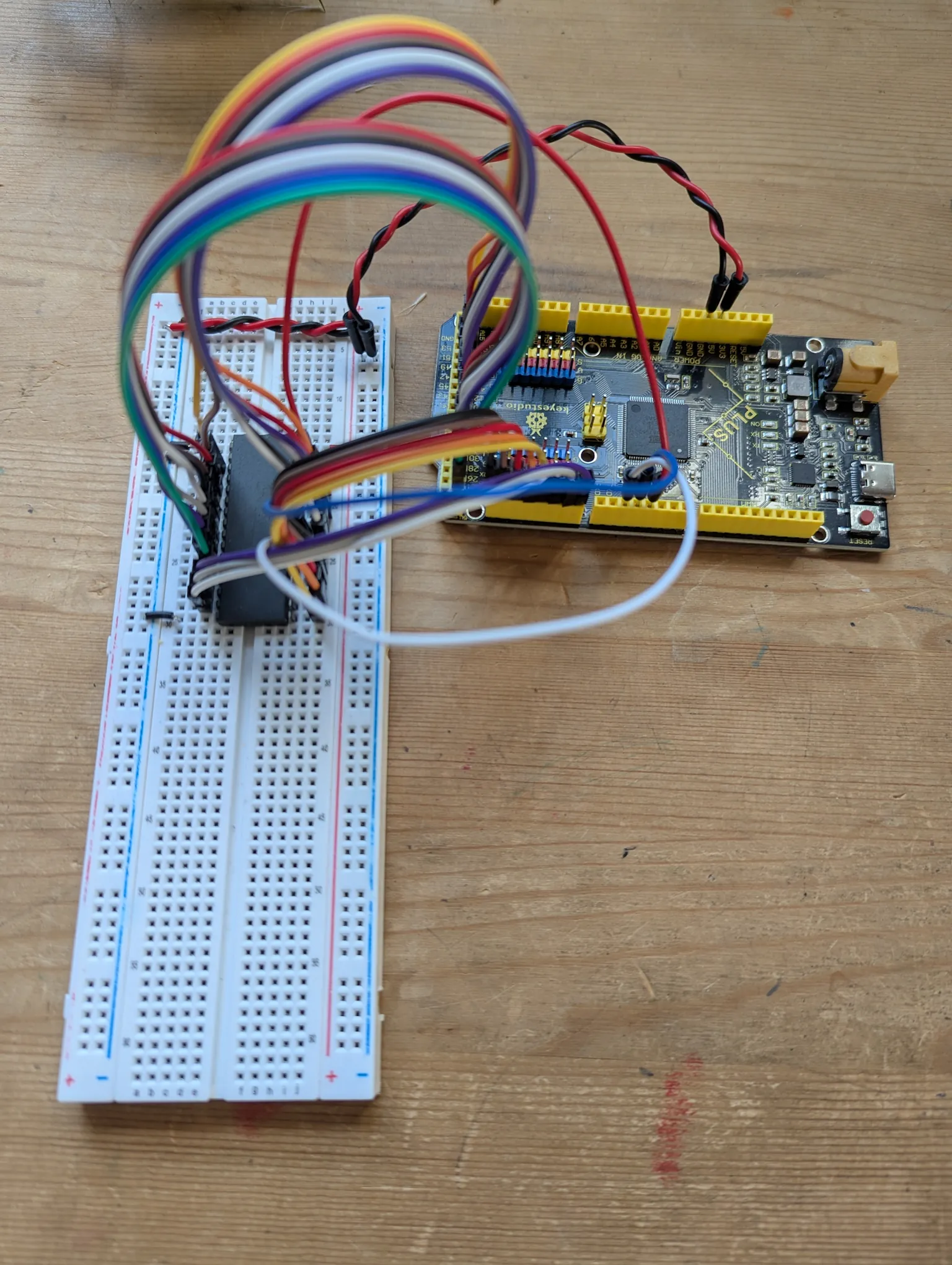
The wiring is done, let's do some basic setup on the Arduino, so that we can specify an address and read or write the data at that location.
//-------------------------------------------------------------------
constexpr uint8_t data_pins[8]      = { 14, 15, 16, 17, 18, 19, 20, 21 };
constexpr uint8_t address_pins[16]  = { 22, 24, 26, 28, 30, 32, 34, 36,
                                        38, 40, 42, 44, 46, 48, 50, 52 };

//-------------------------------------------------------------------
void set_address_lines(uint16_t address)
{
    for (auto pin : address_pins)
    {
        digitalWrite(pin, address & 1);
        address >>= 1;
    }
}

//-------------------------------------------------------------------
void set_data_bus_mode(uint8_t mode)
{
    for (auto pin : data_pins)
    {
        pinMode(pin, mode);
    }
}

//-------------------------------------------------------------------
void set_data_lines(uint8_t data)
{
    set_data_bus_mode(OUTPUT);

    for (auto pin : data_pins)
    {
        digitalWrite(pin, data & 1);
        data >>= 1;
    }
}

//-------------------------------------------------------------------
uint8_t read_data_lines()
{
    set_data_bus_mode(INPUT);

    uint8_t data = 0;
    uint8_t shift = 0;
    for (auto pin : data_pins)
    {
        data |= digitalRead(pin) << shift;
        shift++;
    }

    return data;
}
We will interact with the flash memory in two ways: reading from it, and writing to it. And each of these operations has specific timing requirements that we must comply with. Silicone, to be commanded, must be obeyed.
The chip we have has an access time of 90 ns. When we want to read data, it will be ready 90 ns after our request.
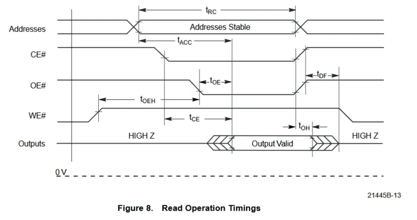
There are only a few symbols of interest here:
| Symbol | Description | Time |
|---|---|---|
| tRC | Min Read Cycle Time | 90 ns |
| tACC | Max Address to Output Delay | 90 ns |
| tCE | Max Chip Enable to Output Delay | 90 ns |
| tOE | Max Output Enable to Output Delay | 35 ns |
Correlating these numbers to the timing diagram, it actually boils down to one thing: by the time we output an address, pull down /CE and /OE, the data will be ready for us at most 90 ns later. And this is our read cycle to account for that:
uint8_t read_cycle(uint16_t address)
{
    set_address_lines(address);

    digitalWrite(chip_enable_pin, LOW);
    digitalWrite(output_enable_pin, LOW);

    // we should wait 90 ns, so at least 2 nops of 62.5 ns each (since we run at 16 MHz)
    _NOP();
    _NOP();

    const uint8_t data = read_data_lines();

    digitalWrite(output_enable_pin, HIGH);
    digitalWrite(chip_enable_pin, HIGH);

    return data;
}
Maybe this could be optimized a bit more, as pulling /OE low probably takes the time that the first _NOP() is waiting for, and we only need to stall 35 ns after the output is enabled, as long as 90 ns has passed since the chip was enabled.
When we want to write data, things are a little different.
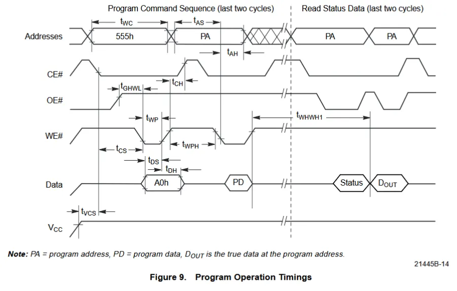
This looks scary, but it is in reality a lot simpler than it looks. When an address and data are on the buses and ready to be sent, we need to pulse the /CE and the /WE signals. The write pulse must be at least 45 ns with our chip. And the chip enable doesn't need to be any longer. Actually, according to the datasheet, their order doesn't even matter. The chip will only latch the address when both signals are pulled down, and it will latch the data as soon as one of them is pulled up. What matters is that we keep 45 ns between these two events to give enough time to the chip to point to the right data. With that in mind, our can code our write cycle like this:
void write_cycle(uint16_t address, uint8_t data)
{
    set_address_lines(address);
    set_data_lines(data);

    digitalWrite(chip_enable_pin, LOW);
    digitalWrite(write_enable_pin, LOW);
    _NOP(); // wait 62.5 ns
    digitalWrite(write_enable_pin, HIGH);
    digitalWrite(chip_enable_pin, HIGH);
}
Reading from the chip is easy: we set the address, wait a little, and read the data. And we do this with a simple call to read_cycle().
Any other operation requires a command. They all start with an unlock sequence. Once unlocked, we can send the actual command to erase a sector, erase the whole chip, program it, or enter the autoselect mode to identify the chip. This last command is used by EEPROM programmers so that they can tell which device they are dealing with.
The secret handshake to unlock the chip is a sequence of two write cycles:
0xaa to 0x5550x55 to 0x2aaThis pattern may look random at first, but it actually looks very intentional. 0x555 is this bit sequence 0101 0101 0101 where every other bit is on. 0x2aa is 0010 1010 1010, same pattern as before shifted to the right. Likewise, the byte we write is 0xaa and 0x55, each other's complement with every other bit on. At this point I'm just guessing, but I think these values are very unlikely to follow each other, making it close to impossible to unlock the chip by mistake and proceed to a destructive operation.
Once the unlock sequence is done, the chip expects the command ID, another byte sent to 0x555 (which complements, again, the address we just wrote to).
Since all commands follow the same pattern, we can write a little function like so:
void send_command(uint8_t command)
{
    write_cycle(0x555, 0xaa);
    write_cycle(0x2aa, 0x55);
    write_cycle(0x555, command);
}
In some cases, we need to send a reset command. Only two cases actually: to get out of the autoselect mode, and to abort a failed write or erase operation. Resetting doesn't require unlocking the device (it is already unlocked when we need it). We just write the byte 0xf0 to any address. And we wait a few milliseconds for good measure.
void send_reset()
{
    write_cycle(0x0, 0xf0);
    delay(10);
}
Let's start with this command. We don't actually need it here, since we already know what our flash device is. But we'll use it to make sure we are able to send commands with a non-destructive operation.
The command id is 0x90, and it puts the device into an autoselect mode until we send a reset. While in this mode, we can retrieve the manufacturer id from address 0, the device id from address 1, and we can also check whether sectors are protected, but we won't bother ourselves with this.
void setup()
{
    // ... initialization code...

    // Identify the ROM
    send_command(0x90);
    auto manufacturer = read_cycle(0x0000);
    auto device = read_cycle(0x0001);
    send_reset();
    print_format("Device: %02x-%02x\n", manufacturer, device);
}
Running this, the result is consistently Device: ff-ff. Not what we expected. The manufacturer is AMD, with a code of 01, and the device is Am29F040B, code a4.
I pulled my hair for a long time trying to figure this out going through the datasheet over and over, experimenting with different timings... I did this for way longer than I want to admit. Until I came to the harsh realization that I had two address lines swapped. A facepalm later, I swap them back, and ta-da! Device: 01-a4. Beautiful!
And by now, this has bit me too many times! When things are not working... Check. The. Wires. Reading a 7f? Check the wires, they're probably shifted one way. Reading fe? Check the wires, they're probably shifted the other way. Reading unexpected results? Check the wires, some may be swapped. This happens very easily with breadboards, tiny connections, and tired eyes. Time to learn the lesson! CTFW!
Now that we can send a command, the rest is going to be a walk in the park. Programming data is the command 0xa0 and it is followed by a write cycle to the destination address with the data to write.
void program_data(uint16_t address, uint8_t data)
{
    send_command(0xa0);
    write_cycle(address, data);

    bool success = wait_for_write(data);
    if (!success)
    {
        print_format("Error Writing %02x at address %04x\n", data, address);
    }
}
Erasing a sector is the command 0x80. It is followed by something that looks a lot like another command, except that the address following the unlock sequence is the sector to erase, not 0x555. We cannot just use send_command() unless we parametrize it with the address, which I'm not willing to do.
void erase_sector()
{
    send_command(0x80);

    write_cycle(0x555, 0xaa);
    write_cycle(0x2aa, 0x55);
    write_cycle(0x0, 0x30);

    bool success = wait_for_write(0xff);
    if (!success)
    {
        print_format("Error Erasing Sector\n");
    }
}
Both programming and erasing call wait_for_write(), which waits until the operation is complete and catches errors. We can never know or assume how long these operations will take, and they can time out. Luckily the chip let us checks the status. To do so, we execute read cycles, and check some data bits. There are two ways to check for success:
While the operation is in progress, we must also check for failures with bit 5. If it's on, an error occurred. In which case we must stop the operation and reset the device. It's more subtle than that, if bit 5 turns on, we have one last chance to check bit 6 or 7 and if they still say in progress, we really have an error. If they don't we're good to go.
It doesn't matter which method we choose since we are checking things programmatically. I picked the #data poll.
bool wait_for_write(uint8_t data)
{
    const uint8_t test_bit = (data >> 7);

    set_data_bus_mode(INPUT);
    digitalWrite(chip_enable_pin, LOW);
    digitalWrite(output_enable_pin, LOW);

    bool success = true;
    while (true)
    {
        int dq7 = digitalRead(data_pins[7]);
        int dq5 = digitalRead(data_pins[5]);

        if ((dq7 == test_bit) && (dq5 == 0))
        {
            break;
        }

        if (dq5)
        {
            dq7 = digitalRead(data_pins[7]);
            success = (dq7 == test_bit);
            break;
        }
    }

    digitalWrite(output_enable_pin, HIGH);
    digitalWrite(chip_enable_pin, HIGH);

    if (!success)
    {
        send_reset();
    }

    return success;
}
Alright, we can erase a sector, program some bytes, and read them! Let's put it all together and actually verify that we are indeed writing and reading properly.
void setup()
{
    // Erase the first sector
    Serial.println("Erasing Sector...");
    erase_sector();

    // Flash some data
    Serial.println("Flashing memory...");
    const char buffer[] = "Frankenstrad 6128";
    const auto length = strlen(buffer);

    for (uint16_t address=0u ; address<length ; address++)
    {
        program_data(address, buffer[address]);
    }

    // Re-read what we just flashed
    Serial.println("Verifying...");
    char test[128] = "";
    for (uint16_t address = 0 ; address < length ; address ++)
    {
        test[address] = (char)read_cycle(address);
    }
    test[length] = 0;

    Serial.print("Source: ");
    Serial.println(buffer);
    Serial.print("Dest  : ");
    Serial.println(test);
}
And the result:
Erasing Sector...
Flashing memory...
Verifying...
Source: Frankenstrad 6128
Dest  : Frankenstrad 6128
We made it! We are able to write data to our flash memory and read them back! Next step is to write some byte code to it, connect it to our Z80 CPU, and have it get its instructions from it.