July 02, 2026
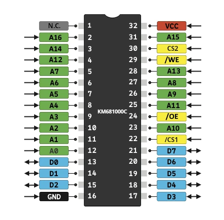
The chip we're using is a static RAM KM681000C with an access time of 70 ns. The pinout is very similar to the ROM chip with one big difference: while the ROM has one chip select active-low signal, this one has two, one active low and another active high. They both need to be active to enable the chip.
ROM and RAM share the same memory space. The ROM is split into a lower bank and an upper bank, which can be independently enabled or disabled. The lower bank occupies the [0000:3FFF] address range, and the upper bank [C000:FFFF]. When a ROM bank is enabled, CPU reads from its range will access the ROM while CPU writes still access the RAM.
We will have eventually to implement the bank switching but for now, with our current setup, the ROM is only going to mapped to [0000:3FFF]. Addresses above will access the RAM. The ROM is already setup to be enabled only when the two highest address lines are off, which is when an address is lesser than 4000h. These two address lines are OR'ed, and the result is OR'ed again with the /MREQ signal coming from the CPU. So the ROM is only active when the CPU is requesting memory and the address is in the range [0000:3FFF]. We are going to need something similar for the RAM which should only be active when the CPU is requesting memory and the address is at least 4000h.
I wasn't too prepared for this, and I only have OR gates and NAND gates. Fortunately, NAND gates are universal gates (like NOR gates), meaning that any logic circuit can be designed with a combination of only NAND gates. It might not be as efficient as using other kind of gates, but it can always be done. The ROM already has a signal for when the address is in the range [0000:3FFF]. We can invert that signal and combine it with the /MREQ signal to enable our chip. And we will invert the result to get the opposite signal we also need.
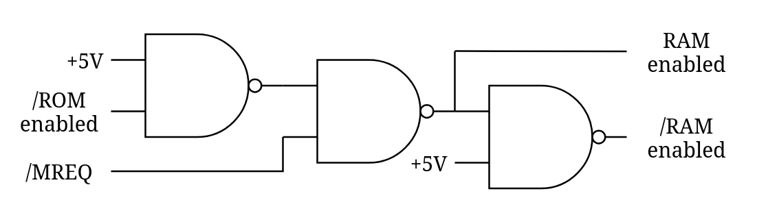
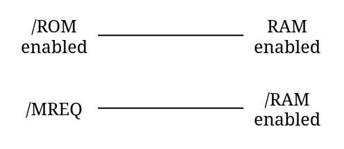
Looking at this diagram, I realize that there is a much simpler design. Both signals must be active but they don't have to be bound to each other. The active low can just use the /MREQ signal, straight from the CPU. And the active high can just be the inverted ROM enabled signal. It is even simpler than that, since the ROM enabled signal is passive low, we can wire it straight to the active high RAM enabled signal. The same signal will turn on the ROM while turning the RAM off and vice-versa. This is perfect, we are using half a dozen less wires and we no longer need NAND gates. We have an elegant solution that should still work when we emulate the gate array to switch between ROM and RAM.
Both RAM and ROM are now plugged in. Up until now, the ESP32 was emulating the RAM, we are going to stop that and let the real RAM do its part. The clock routine on the ESP32 has to change. It still needs to sample the address bus all the time, and it will keep sampling the data bus during write operations so that we know what data is sent to memory. But we are going to disable any read operation, since from now on the system will only read from the ROM or the RAM.
void IRAM_ATTR on_z80_clock()
{
    z80_clock_state = 1 - z80_clock_state;
    gpio_set_level(clock_signal_pin, z80_clock_state);

    if (z80_clock_state == LOW)
    {
        // Falling edge of the clock: sample the address bus
        address_bus = 0;
        int shift = 0;
        for (const auto line : address_lines)
        {
            address_bus |= gpio_get_level(line) << shift;
            shift ++;
        }
    }
    else
    {
        // Rising edge of the clock
        if (gpio_get_level(_read_pin) == LOW)
        {
            // Disable the data lines when reading
            for (const auto pin : data_lines)
            {
                gpio_set_direction(pin, GPIO_MODE_DISABLE);
            }
        }
        else if (gpio_get_level(_write_pin) == LOW)
        {
            // Sample the data lines when writing
            uint8_t data = 0;
            int32_t shift = 0;
            for (const auto pin : data_lines)
            {
                gpio_set_direction(pin, GPIO_MODE_INPUT);
                data |= digitalRead(pin) << shift;
                shift++;
            }
            memory[address_bus] = data;

            write_signal = true;
        }
    }
}
And to test this, we are going to adapt our little program. It is still going to read a string from the ROM and write it back in RAM. But then it will read the same string we just wrote in RAM and write somewhere else in RAM. The ESP32 doesn't know what is read, but it knows what is written. So the second copy will show us whether the first copy worked, and if we were able to write in RAM. Ideally, a third copy would also show us whether reading from RAM (during the second copy) also works, but I'm feeling lucky! We're just going to trust that if we can write in RAM, we can read from it. As I'm writing this down, I realize how big of gamble this is, but again, I'm feeling lucky!
uint8_t rom[] =
{
    // Code
    0x21, 0x20, 0x00,       // LD HL, 0020h
    0x11, 0x00, 0x40,       // LD DE, 4000h
    0x01, 0x13, 0x00,       // LD BC, 0013h
    0xED, 0xB0,             // LDIR

    0x21, 0x00, 0x40,       // LD HL, 4000h
    0x11, 0x00, 0x60,       // LD DE, 6000h
    0x01, 0x13, 0x00,       // LD BC, 0013h
    0xED, 0xB0,             // LDIR

    0x76,                   // HALT

    // Padding
    0x00, 0x00, 0x00, 0x00, 0x00, 0x00, 0x00, 0x00, 0x00,

    // Source Data "Frankenstrad 6128"
    0x46, 0x72, 0x61, 0x6E, 0x6B, 0x65, 0x6E, 0x73, 0x74, 0x72, 0x61, 0x64, 0x20, 0x36, 0x31, 0x32, 0x38, 0x00
};
In the ESP32 main loop, we just output what we have in our mirrored memory:
void loop()
{
    if (write_signal)
    {
        write_signal = false;
        Serial.printf("WR [%04x] [%02x]\n", address_bus, memory[address_bus]);
        Serial.printf("4000: %s\n", &memory[0x4000]);
        Serial.printf("6000: %s\n", &memory[0x6000]);
    }
}
And just like that, CPU, ROM, and RAM are dancing together to the beat of the ESP32!
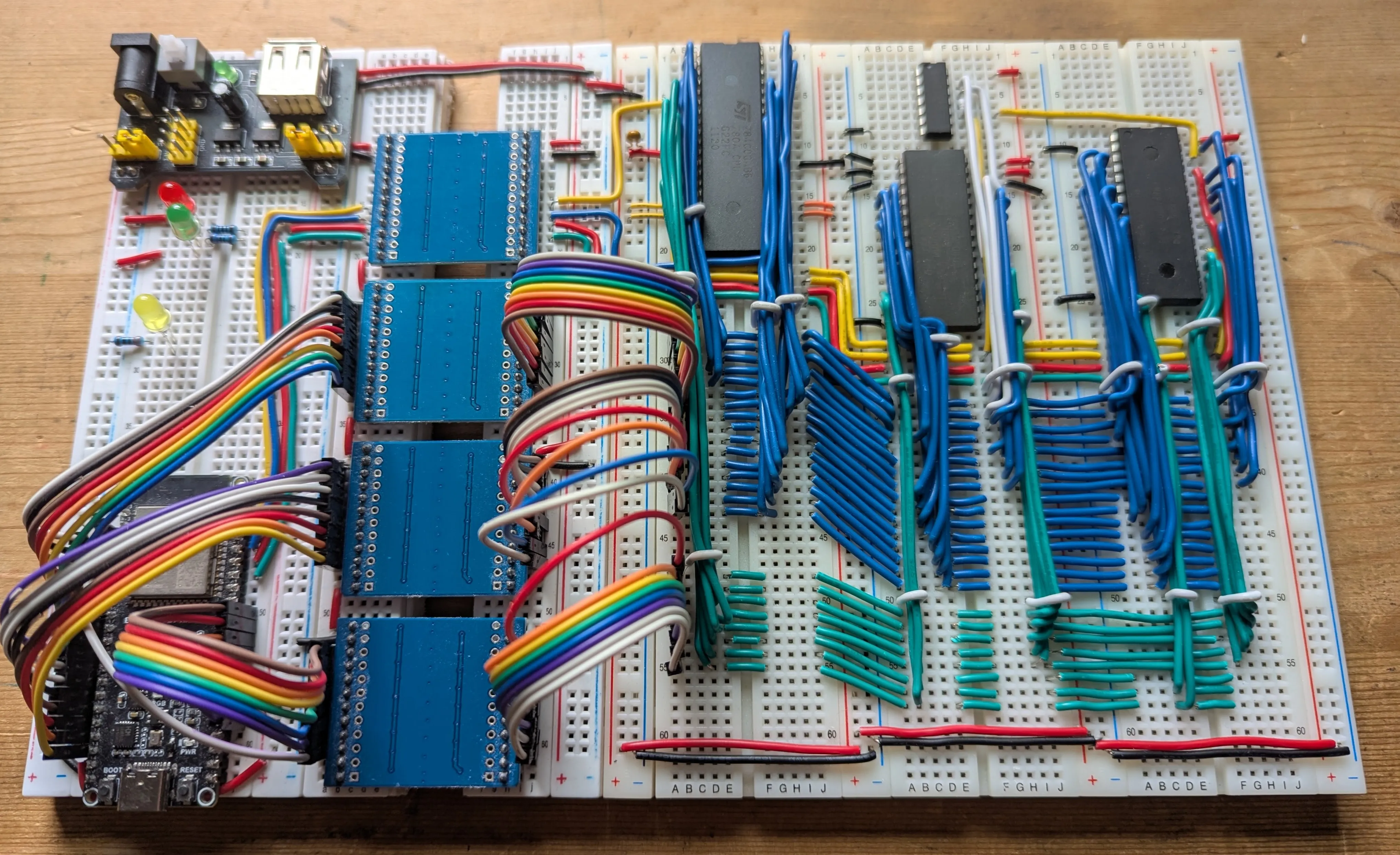
At this point, the ESP32 is only pulsing the clock signal and spying on the write operations. Looking at these is the only reason why it is wired to the complete address bus, and this is starting to be a problem. There is no more room left for other signals. There are options to change the 16-bit address lines to use fewer GPIO on the ESP32, but that's not really the point. The ESP32 will have other things to do, like emulating the gate array at a decent speed, and it should only look at the top two address lines, like the gate array does in order to enable ROM and RAM accordingly.
The scary part is that so far, the ESP32 was our ears and eyes to know what is going on in our system. But we need to let it go and this is giving me crazy separation anxiety. So, moving forward, we will use the Arduino Mega to spy on the system. It has plenty of pins to look at the address, the data, and various control signals. And it has nothing else to do, except on the rare occasions when we need to flash the ROM. And it will free the ESP32 to do what it got to do.
But that will be in a while because I'm going away for a few weeks. And this is also giving me separation anxiety. Learning through this project while giving in to nostalgia is bringing me much joy and I will miss tinkering with it. But that's not the real reason. My fear is to forget where I was at and what to do next. Hopefully I will be able to pick up where I left with these articles and the code repository...
So maybe it's a good idea to write down what's next and spread some bread crumbs over the breadboards. I have three candidates:
So this is what we will do:
There, I feel much better now that I have a plan! And on that note, peace out! ✌️