August 12, 2026
There was a small list of things to fix up before we continue the journey. Let's go through them, it won't take long.
It's not that the application just renders garbage on the screen; it often crashes. Apparently, the compressed data we receive is corrupted and way bigger than expected.
Because the UDP packets are so big, they bust the MTU and get fragmented. Decompressing the packets crashes because the buffers are incomplete. The fix is easy: send the overall size uncompressed first as a header of the data, and keep receiving packets until we got everything. Only then decompress.
That fixes the crash, but the frame data is still garbage. A closer look at the ESP32 code reveals a bad pointer indirection. I was not sending the content of frame buffer but some random memory (the content of the stack to be specific). Fixing the indirection fixes the display. A silly mistake I introduced while "cleaning up" some code.
There! All good! We can get mesmerized again by the little yellow ball bouncing off the edges of the screen.
So the ESP32 is running out of GPIOs. Lucky for us, it is not actually supposed to read all sixteen address lines from the system, but only the two last. This was just a temporary thing to fake the RAM. Now that we have both ROM and RAM wired up, we don't need this anymore.
But we were using it to also monitor the reads and writes in memory. This crutch was helping us get a sense of what the system is doing and we need a replacement. This replacement is going to be our Arduino Mega which is collecting dust most of the time.
This is very simple. We connect the Arduino's GPIOs to the address bus, the data bus, and our signals, specifically the /RD and /WR signals. When something is read or written somewhere, we can output the address and data to the serial monitor. Maybe later we check if we are running the Z80 machine cycle and decode the instruction to display it. But for now, just outputting the writes will do!
Now that the ESP32 is not looking at the whole address bus, we can dedicate its GPIOs to act more like the CPC Gate Array. It is going to replace the logic gates that enable and disable the ROM and the RAM. But to do that, we have a bit of rewiring to do.
So far, we had CPU signals going across the system to notify of memory requests and whether they were reading or writing. The gate array should be handling this, as we can see in the CPC circuit diagram. We are going to redirect these signals to the ESP32 which will combine them into simpler signals for the system: read from ROM, read from RAM, and write to RAM. But while we're at it, we are going to send all the CPU signals to the ESP32, because eventually it is going to need most of them to drive the whole system like the gate array does.
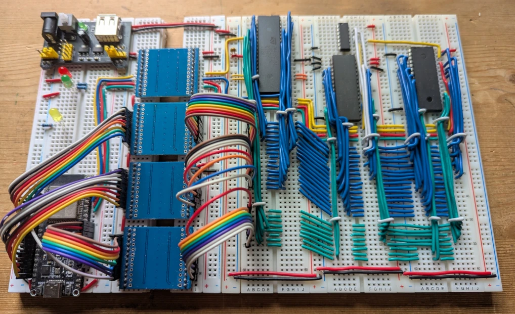
Rewiring the signals is not that simple though. Since the wires are trapped under the address and data bus wires and we will have to redo the buses as well.
We pretty much have to rewire the entire system. What I thought was going to be a "little" rewiring has quickly escalated into a major rewiring! But that's for the best. I came to realize that the Z80, the ROM, and the RAM pinouts all have something in common: the data pins are on one side of the chips while the address pins on the other.
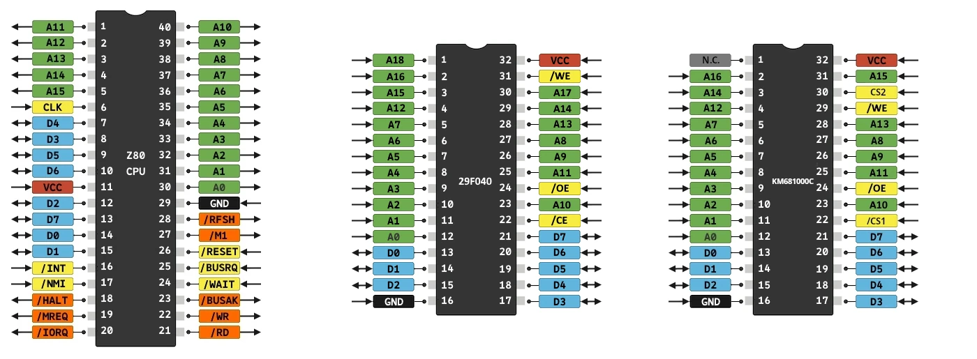
This is not random and it makes a lot of sense for our breadboard setup. If we keep the address bus on one side and the data bus on the other, we can come up with a cleaner design with shorter and non overlapping wires. This is going to look much nicer!
A few hours later, after much wire clipping, stripping, and bending, here is the new system (Arduino spy included)!
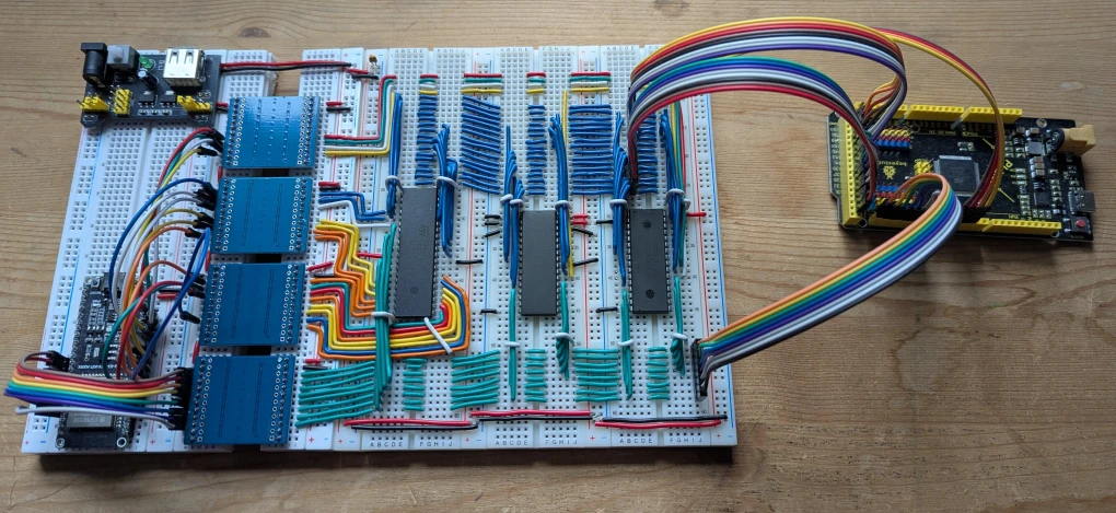
The address lines, in blue, are "above" the chips. The data lines, in green, are "below". The CPU signals are all going to the left into the ESP32 realm. On the other side of the level shifters, the signals are plugged with jumper wires. I have a feeling these connections will change overtime and jumper wires will be easier to switch around. At the top of the boards, "above" the address lines, we have four new lines: one to enable the ROM, one to enable the RAM, one to read, and one to write. There is room for more signals we will add later on for IO requests and memory access arbitration (so that CPU and video chip can take turns accessing the RAM).
The rightmost chip is the RAM. It won't be directly accessed but guarded behind multiplexers which will alternate the access between the CPU and the video chip. Before we add more chips to the system, we are going to set up the multiplexers and complete our memory module, then we will be ready for the video chip.