August 25, 2026
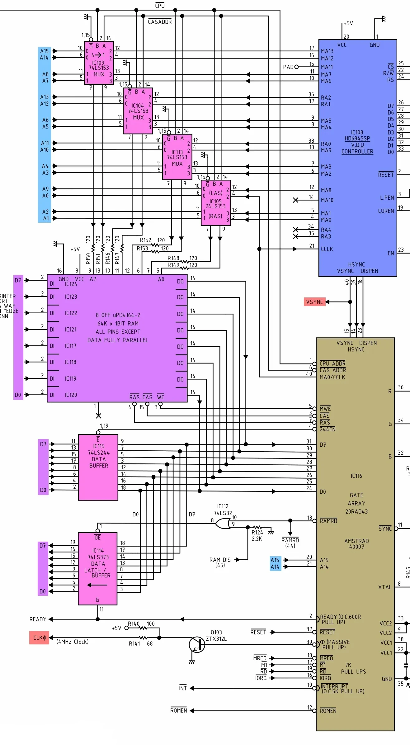
So far, we've been using the RAM as simply as possible. We wired it to the address bus and the data bus and the ESP32 was just sending the read and write signals. But the actual CPC is more complex, with a RAM module comprising three parts:
PD4164 DRAM chips. Each chip holds 64 kbits and only deals with one bit at a time. They are parallelized to get to 64 kbytes.74LS153 chips arbitrate the memory access between the CPU and CRT Controller and split the 16-bit addresses into two 8-bit words, row and column, to address the DRAM since that's what the DRAM chips expect.74LS244 is a data buffer and it allows the signal to flow in one direction only.74LS373 is also a unidirectional data buffer, but it can latch the data as well.
The design of the Frankenstrad is different though. Instead of eight DRAM chips, we are using one single SRAM chip KM681000C. This is going to change a few things:
74HCT245 data buffers for this. Two for the CPU address bus and two for the CRTC. And we are going to enable them to grant access to one side or the other.74LS244 is going to be changed to a 74HCT245. Technically a 244 would do, but the 245 pinout is easier to work with as all the pins for the same port are on the same side of the chip. The 245 is bidirectional, but we'll enable only the one direction we need. Since it is now guarding the RAM's data pin, it needs to be enabled when we write to the RAM.74LS373 is going to be changed to a 74HCT373. For now only the CPU is connected to it, so we can just latch the data all the time. When the CRTC will come into play and for slow I/O operations we will stop latching until we're ready. Its output is only enabled during read operations.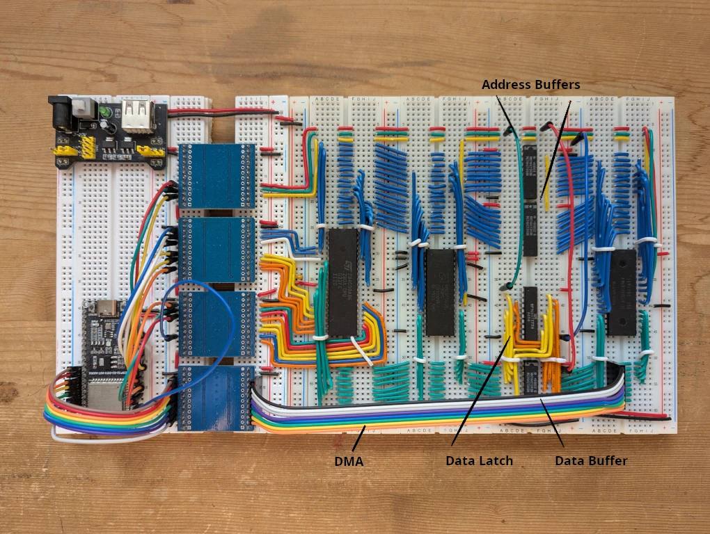
I made it sound like these modifications are simple, but that's a lie. Up until now, I've been following the circuit diagram. But a different RAM calls for different supporting chips. And, without fully understanding yet what the gate array does, I'm only guessing what these supporting chips are doing. And figuring out this new design takes a lot of trials, errors, and monitoring.
At first, I had both the data buffer and the data latch enabled at all times. Both chips were feeding off each other with a highly unstable result that ended up sitting on the bus when reading or writing. We start a read, bits are coming out from the RAM, they're latched right away and sent back to the data buffer, possibly conflicting with other bits still coming out of the RAM, on the same wires, latched again, and so on and so forth. Both chips are basically crossing the streams, which, as we know, should never be done!
I had to debug the system to understand that. Until now, the monitoring program was only looking at the write operations, but I needed to also look at the read operation to properly troubleshoot the memory module. The read operations include reading the instruction op codes though. That's a lot of "noise" when we just want to look at the memory operations.
Lucky for us, the CPU has a /M1 signal. The active low signal goes low during the machine cycle, which is when the opcode is fetched from memory and executed. The cycles that are not the machine cycles are the actual reads and writes from memory or I/O. And that's the ones we're interested in.
This is the new monitor loop that only displays what we want, free of opcode reads:
void loop()
{
    const bool write = digitalRead(_write_pin) == LOW;
    const bool read = digitalRead(_read_pin) == LOW;
    const bool m1 = digitalRead(_m1) == LOW;
    if (!m1 && (read || write))
    {
        BusState state;
        state.read = read;
        state.write = write;
        state.address = read_address_bus();
        state.data = read_data_bus();

        if (state != last_state)
        {
            print_format("%c %04x: %02x '%c'", read ? 'r' : 'W', state.address, state.data, state.data);
            last_state = state;
        }
    }
}
Seeing exactly what is read, from where, and what is written is really helpful, because then I can see when the system stops working and where by moving the data probe along the bus. And the solution is obvious: only enable the data buffer when writing, only enable the data latch when reading, and, at least for now, always latch the data.
We're getting there! Only 3 important chips to go: the CRTC, the PIO, and the sound chip. Once this is all wired, we can flash the ROM with the CPC BIOS, and execute it! Or at least try... At that point, our Z80 is going to run a whole bunch of instructions. It's going to do a lot of crazy stuff and I'm expecting a lot of hiccups.
Seeing what it's doing is going to be crucial. To that end, we are going to give our monitor an upgrade and have it look at the machine cycles and print out what instructions are being executed.